マイクロLED、LED、VCSEL(垂直共振器型面発光レーザー)、検出器およびフォトニクス
化合物半導体オプトエレクトロニクス用ALDソリューション
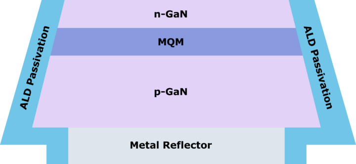
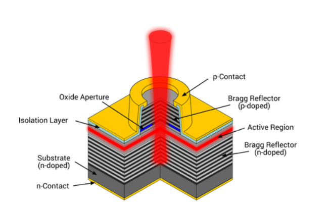
GaN(窒化ガリウム)、GaAs(ヒ化ガリウム)、InP(リン化インジウム)など複数の元素を組み合わせた化合物をベースとしたデバイスは、その技術の進歩に伴い、より精密で柔軟な製造工程を必要としています。ALD(原子層堆積法)は、次世代のオプトエレクトロニクスに必要なサイドウォールパッシベーション、サーフェスパッシベーション、ファイナルパッシベーション、そして反射防止コーティングなどを可能にします。
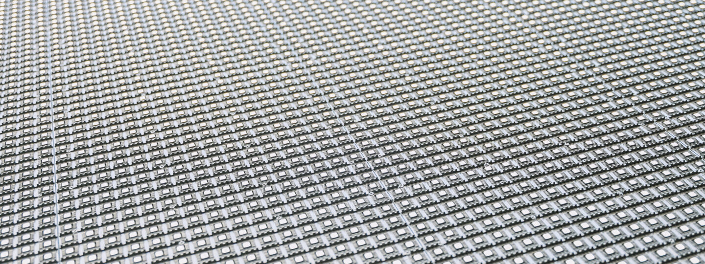
microLEDのような新しい半導体フォトニックデバイスは、これまで既に確立されてきた技術よりも多くの性能向上をもたらしています。ウェハレベル技術への移行に伴う高度なデバイスのアーキテクチャと小型化は、プロセス技術と製造上の課題を新たに生み出しており、その普及を遅らせています。ALD(原子層堆積法)は、こういった厳しい設計要件を満たし、マイクロLED、VCSEL、その他の化合物半導体オプトエレクトロニクスデバイスの大量生産を可能にするために必要な適合性、材料の柔軟性、膜機能を兼ね揃えています。
LED&フォトニクス用ALDソリューション
プロセス
サーマルALD (Thermal ALD)
プラズマALD (Plasma-Enhanced ALD)
原料
Al2O3, AlN, SiO2, Si3N4, HfO2, ZrO2
基質
GaAs, InP, GaN (InGaN, AlGaInP), AlN
3, 6, 8, 12″ ウェハ
ALDは製造の効率化、光強度の向上に加えて化合物半導体オプトエレクトロニクスにおける確実性を上げる手段として昨今急速に成長しています。当社のプラズマALDおよびサーマルバッチALDクラスターツールで実現する、等角性かつ高密度、高いバリア性(ピンホールフリー)を持つALD成膜には下記のような特徴があります。
- メサ構造などに用いられる、等角なサイドウォールパッシベーション
- ファイナルパッシベーション用高品質フィルム
- 調整可能な酸化物ベースの分布ブラッグ反射鏡(DBR)の製造
- 放熱用誘電体層
- 透明導電性酸化物の蒸着
LED&フォトニックデバイス市場についてもっと詳しく
III-V族半導体の詳細とオプトエレクトロニクスでの使用についてはこちら
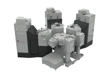
Prodigy
Beneq Prodigy™は、化合物半導体やMEMSの大量生産向けのシンプルでかつ手際の良いALDソリューションです。
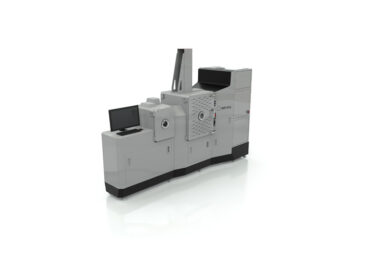
Transform®
Beneq Transform®は、電子機器、MEMSおよびセンサー、RF、LED、フォトニクス、高度なアプリケーションパッケージなどが1つのプロダクトで実現可能なALDソリューションです。