ALD solutions for compound semiconductor optoelectronics
Advances in GaN, GaAs, and InP –based devices continually demand more precise and flexible manufacturing solutions. ALD enables conformal sidewall passivation, controlled surface passivation, final passivation, and anti-reflective coatings necessary for next generation optoelectronics.
ALD FOR LED & PHOTONICS
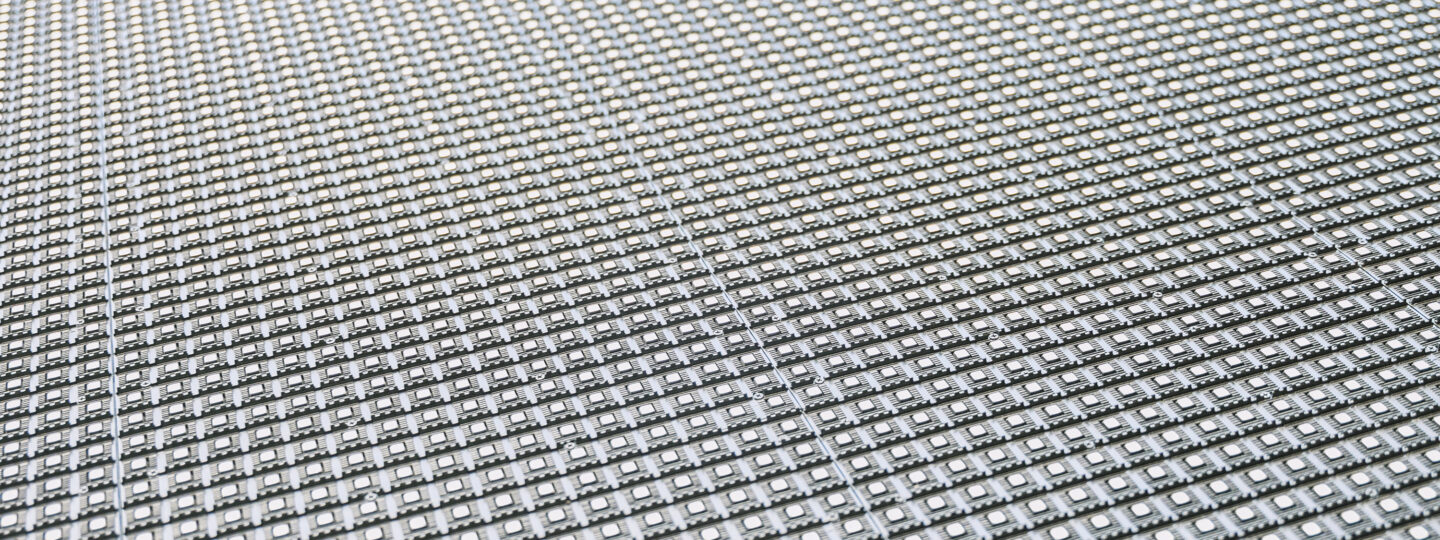
Emerging semiconductor photonic devices, like microLEDs, offer many performance improvements over well-established technologies. Advanced device architectures and miniaturization accompanying the shift to wafer-level technology also create process technology and manufacturing challenges that delay widespread adoption. Atomic Layer Deposition offers the necessary conformality, material flexibility and film functions to meet these strict design requirements and enable high volume manufacturing of microLEDs, VCSELs and other compound semiconductor optoelectronic devices.
ALD is rapidly growing as a means to improve efficiency, light intensity and reliability in compound semiconductor optoelectronics. Conformal, dense, pinhole-free films ALD films and controlled interfaces enabled in our sequential plasma-enhanced and thermal batch ALD cluster tools offer:
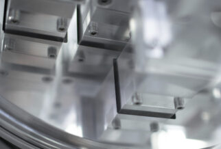
Conformal sidewall passivation for, e.g. MESA structures
Miniaturization of LED technology requires a shift to more precision deposition techniques to enable mass production. With ALD, display manufacturers can reliably improve yield, efficiency, and lifetime of their MicroLEDs.
Perpendicular operation geometry has simplified VCSEL manufacturing processes compared to traditional edge-emitting lasers. Atomic layer deposition offers sub-nanometer control for precision fabrication of VCSEL architecture.
III-V semiconductors are a unique class of materials that are made up of elements from the third and fifth columns of the periodic table. Learn why these compounds are interesting and their applications in optoelectronics.
ALD offers the only way to create conformal ultra-thin protective coatings on surfaces with high aspect ratios and complex 3D shapes. ALD is also a great solution for encapsulating sensitive surfaces. Here are 3 of Beneq’s ALD moisture barrier customer cases from the electronics industry.
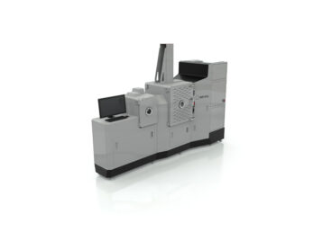
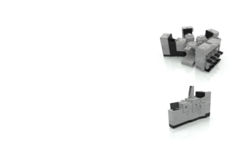
Beneq’s high-capacity ALD solutions have enabled completely new innovative products and coatings that have not been possible in industrial scale before. The reason is simple: Beneq has taken deposition speed, capacity and throughput of ALD equipment to a completely new level. Today, we start a throughput revolution for ALD in new More than Moore wafer processing markets.
One of the classic mistakes of engineer-driven high tech companies is to assume that people – customers, partners, website visitors, journalists – understand the benefits of the technology when they see it. The advantages of having an ALD-based bottom DBR in LEDs are obvious, right? Everybody gets that.
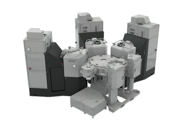
Ever since we earlier this year announced the licensing of rotary spatial ALD technology and launched Beneq R11, our new rotary tool for plasma enhanced spatial ALD, we have received a steady flow of inquiries and questions about where we see the new equipment being the most useful.
We are introducing two new products that move the capacity of industrial ALD equipment to the next level. As Tommi says in our news release, our target is to revolutionize the coating speed standards in the ALD industry. When it comes to ALD coating throughput, m2 is the new mm2.
Earlier we shared examples of industrial use of ALD in moisture barriers. Now we continue with another typical area of ALD applications: Optical coatings.
Earlier today we shared news about the next solution in our spatial ALD equipment family: A new rotary spatial reactor we are developing based on technology we have licensed from Lotus Applied Technology.