VCSEL
Manufacturing VCSELs with ALD
Perpendicular operation geometry has simplified VCSEL manufacturing processes compared to traditional edge-emitting lasers. Atomic layer deposition offers sub-nanometer control for precision fabrication of VCSEL architecture.
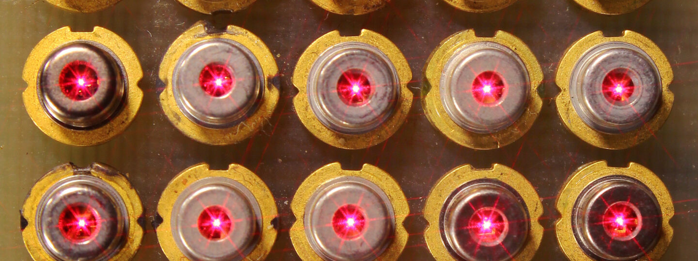
Vertical-cavity surface emitting lasers (VCSELs) represent a breakthrough in optical technologies, allowing laser photons to be directed perpendicular to the device surface rather than parallel. The new emission geometry brings numerous advantages including low beam divergence, easier integration with other optical components, e.g. collimating lenses, and the ability to test the device on-chip without needing to cleave the wafer. The device set up has simplified VCSEL manufacturing processes, allowing for 2-dimensional arrays of lasers to be fabricated.
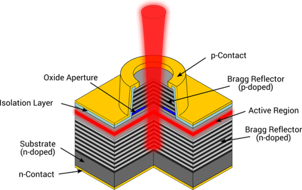
VCSELs are a semiconductor device, typically made on a gallium arsenide substrate, with a recognizable architecture of a quantum well sandwiched between two distributed Bragg reflectors (DBRs). The quantum well acts as the region where most of the lasing occurs, while the DBRs are strategically designed to induce constructive interference of laser photons and reflect light through the aperture. VCSELs have found widespread use in optical communications, storage, and more recently, LiDAR.
Fabricating high-contrast optical stacks
Atomic layer deposition is an excellent technique for fabricating several components in a standard VCSEL. In particular, the wide range of materials available with ALD and the precision thickness control offers a simple fabrication method for single or multilayer optical stacks. It can be used for depositing high-contrast stacks with tunable optical properties, like those needed for antireflective coatings or oxide-based DBRs.
ALD may also be used in the VCSEL manufacturing process for:
- Conformal surface passivation of MESA structures
- Embedded current confinement apertures
- Heat dissipation layers
Explore our other applications of ALD for LED & Photonics!