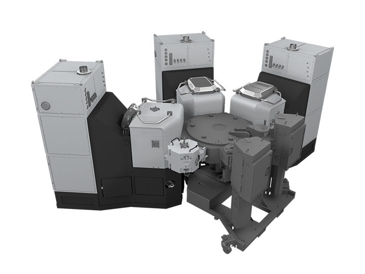
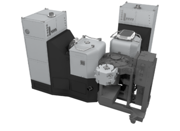
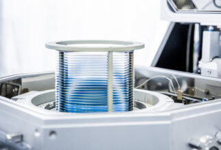
The brand-new cluster design offers customers unparalleled flexibility by combining both thermal and plasma ALD with single wafer and batch processing, on a single automated platform.
Atomic Layer Deposition (ALD) is an unmatchable moisture barrier and encapsulation solution for electronics and semiconductor components. The ultra-thin ALD moisture protection can be applied in different phases of the production process: wafer-level, chip-level, package or module-level, and/or Assembled Printed Circuit Board (PCBA) level.
ALD offers the only way to create conformal ultra-thin protective coatings on surfaces with high aspect ratios and complex 3D shapes. ALD is also a great solution for encapsulating sensitive surfaces. Here are 3 of Beneq’s ALD moisture barrier customer cases from the electronics industry.
Beneq is on a mission to introduce ALD to a whole new set of industrial applications. Earlier, we have talked about fast ALD, spatial ALD solutions and next generation ALD equipment that changes the standards of throughput for industrial ALD production. Next, our plan is to start a throughput revolution in ALD for the semiconductor industry.
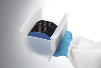
Today, we would like to talk about how our expertise in high-capacity ALD is benefiting our customers in wafer research and industrial wafer-processing in markets with high throughput requirements, such as the semiconductor, MEMS and LED industries.