TECHNOLOGY
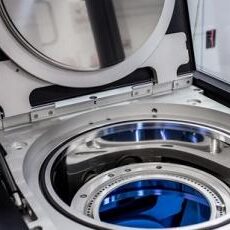
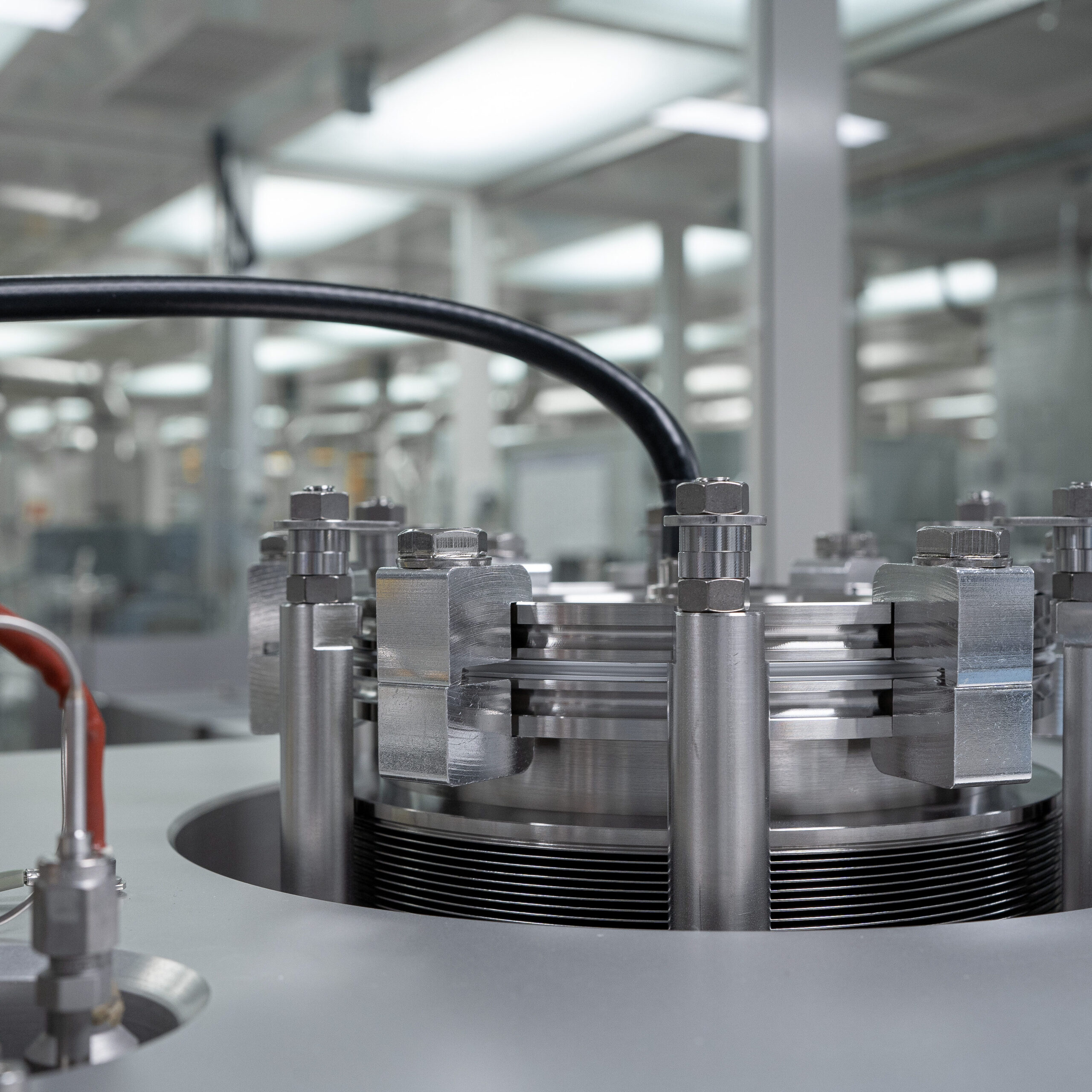
Atomic Layer Deposition
What if you could manipulate matter at the nano scale? What if you could build things up a layer of atoms at a time? Wonder no more. Welcome to Atomic Layer Deposition.
What is Atomic Layer Deposition?
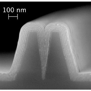
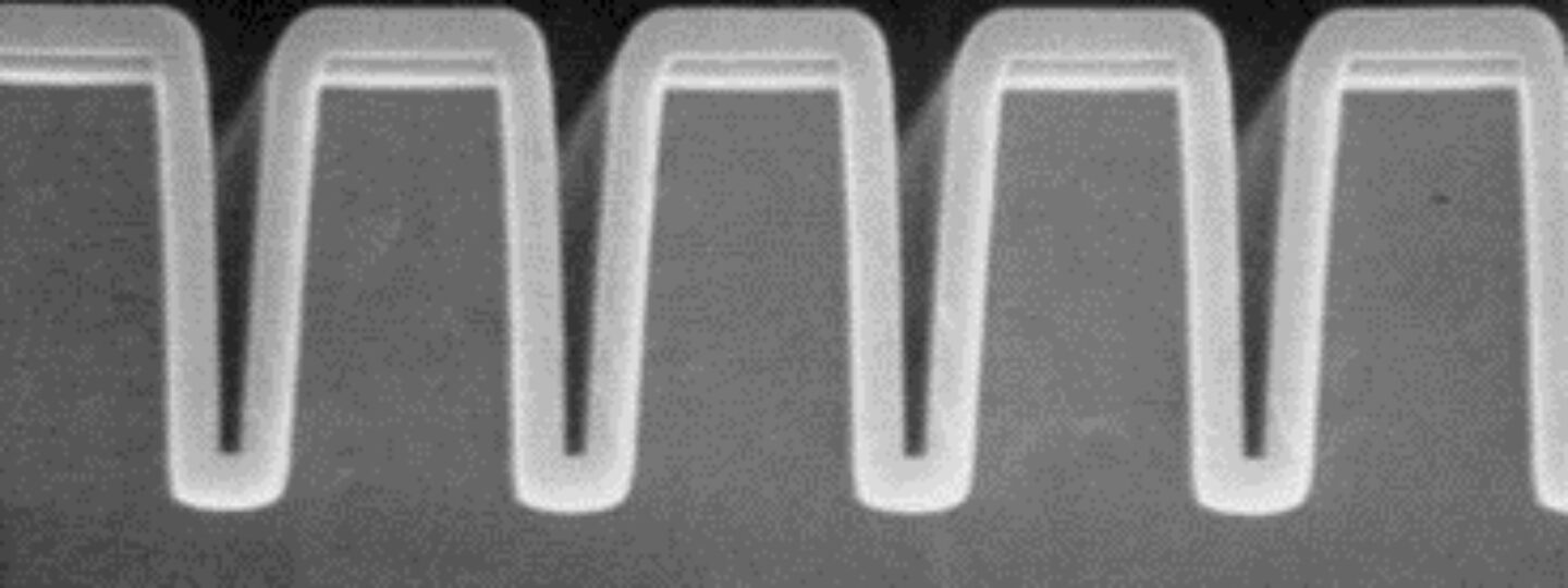
Atomic Layer Deposition (ALD) is a thin film deposition technique enabling the fabrication of next-generation devices across the globe’s most innovative industries. Used to manufacture high-quality coatings with Angstrom-level precision and conformality unrivaled by other deposition technologies, ALD has become a necessary coating tool for the advancement of nanotechnology.
Originally developed to manufacture phosphor films for electroluminescent displays, ALD became an integral enabling technology for chip miniaturization in the semiconductor industry. It is one of the sole, and often unrecognized, reasons modern electronics are as fast and powerful as they are.
Today, ALD continues to bear fruit for semiconductor manufacturing and is becoming mainstream in countless new industries from optics, photonics and image sensors to MEMS, green energy and jewelry. Each year more papers on ALD are published than the last and unique applications for conformal thin films are discovered. We are only beginning to scratch the surface of what is possible with Atomic Layer Deposition.
Atomic Layer Deposition Benefits
The precision nature of the ALD process provides numerous benefits. Some advantages include:
Check out this page for more information on how ALD compares to other thin film deposition processes!
How does ALD work?
ALD is based on a binary sequence of self-limiting surface reactions which builds up a film of solid material with Angstrom-level control. It operates in cycles of alternating reactions with one ALD cycle depositing one “atomic layer.” The thickness of the resulting film is directly dependent on the number of ALD cycles performed, giving high control over the film growth.
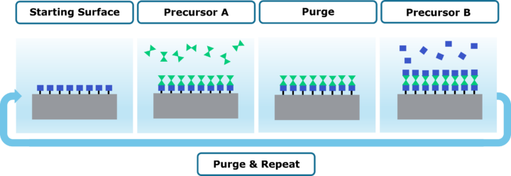
During an ALD reaction, precursor molecules react with sites on the substrate surface. Once all available surface sites have become occupied, or saturated, the reactions “shut off” on their own. By driving reactions to completion every time, the resulting films are highly conformal and have a very low amount of defects. This self-limiting aspect is the cornerstone for ALD’s unique power.
Watch this video to learn more about ALD!
Take a closer look at Atomic Layer Deposition