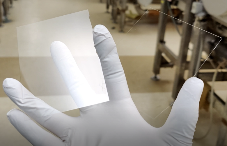
What is Thin Film Deposition?
Thin film deposition is the process of building material on substrates in the range of a couple nanometers up to about 100 micrometers. There are several types of thin film deposition with each technology having different characteristics for how sources are vaporized, how quickly they deposit material, available materials, and resulting film properties.
Thin film deposition can be broadly split into chemical methods and physical methods. Chemical methods deposit materials via chemical reactions at the surface while physical methods mechanically or thermally create sources for films. Chemical vapor deposition, or CVD, is one of the most commonly used chemical methods where gaseous precursors react or decompose to deposit a film. Physical methods are quite broad and typically referred to as physical vapor deposition, or PVD. PVD is often split into evaporation and sputtering processes.

ALD vs CVD

Atomic layer deposition (ALD) is a type of CVD method with high precision. Both utilize chemical reactions to deposit thin films, but ALD utilizes reactions that are controlled at the surface, rather than by flux. By separating the individual reactions in an ALD process, it allows much higher control of the film thickness, density and conformality. This makes ALD a much preferred method for depositing very thin films (10-50 nm) and/or on high-aspect ratio structures ( > 10:1). CVD is preferable for depositing thick films at high deposition rates. CVD also has a much wider range of available precursors since decomposition is a valid pathway.
ALD vs PVD
PVD methods, like sputtering, operate quite differently than ALD and other CVD processes. For example, in sputtering, a high energy beam will bombard a source material and send atoms on a path to the substrate where it condenses on the surface. The main difference here is the deposition is “line-of-sight” meaning only surfaces which are directly in the path of the source will be coated. ALD is an isotropic process so all surfaces are coated equally. PVD works well for low temperature processes and alloy depositions, especially at high deposition rates and on simpler substrate geometries.

Below you can find a high level comparison between ALD, CVD, and PVD.
Thin Film Deposition Method Comparison
