OPTICAL COATINGS
Conformal thin films for curved and freeform optics
Emerging optics, such as those in mobile phone cameras, AR/VR goggles and LiDAR devices, reach the limits of traditional PVD technologies and demand optical coatings with conformality only achievable by ALD.
OPTICAL COATINGS BY ALD
Coating complex optics made easy. Current optical coating methods are well-established for low cost, tolerable process temperature and high throughput. However, traditional PVD coating technologies lack high conformality, making emerging microstructured, curved and freeform optics difficult to coat. For coating complex optics, atomic layer deposition provides advantages over PVD, like precise thickness control and uniformity, without sacrificing film performance.
Process Options
Thermal ALD
Plasma-Enhanced ALD
Materials
SiO2, TiO2, Al2O3, HfO2
Ta2O5, Nb2O5, ZnS, Si3N4,
Substrates
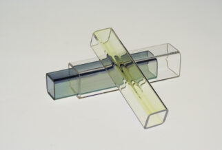
Lenses, fibers, domes, waveguides, freeform
OPTICAL COATING SOLUTIONS
At Beneq, we have optimized conformal optical coating deposition at the intersection of uniformity, batch size and deposition rate. ALD is suitable for all types of optical coatings including:
- Antireflective (AR) optical coatings
- Highly reflective and highly absorbing coatings
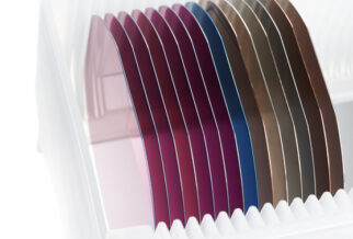
- Bandpass, bandstop and edge-pass filters
- Waveguide cladding, core or strain layers
- Transparent conductive oxides
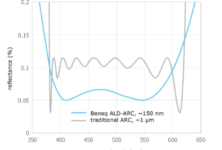
Antireflection Coatings
Antireflective coatings are the most common type of optical coating. Learn about the benefits of fabricating ARCs with ALD and Beneq’s innovative ARC solutions.
Read more about Antireflection Coatings>
OPTICAL COATING EQUIPMENT
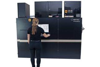
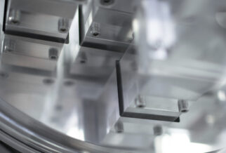
BENEQ P400A
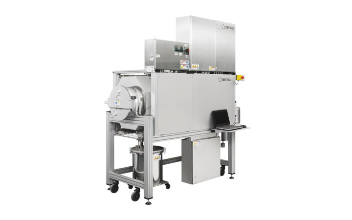
Designed for the perfect balance between uniformity and throughput. Despite a lower deposition rate than PVD, ALD enables you to coat your optics in much larger batches. ALD processes coat entire components conformally, giving you unparalleled uniformity and throughput compared to PVD.
The Beneq P400A is optimized at the intersection of uniformity, batch size, and deposition rate to deliver you the highest quality thick films. We provide you with expertise and software to design every individual ALD layer for the best performance in the context of your design constraints.
Learn more about Beneq P400A >
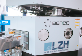
BENEQ C2R
Ultra-fast high precision spatial ALD coatings. Beneq C2R provides an optimal solution for high throughput ALD in volume production of optical coatings. With deposition rates up to 1 µm/hour and plasma capabilities, the Beneq C2R is the ideal product when speed, cost, low process temperature, and the highest possible film quality are the driving factors.