POWER DEVICES
ALD Interface Engineering for Silicon Carbide (SiC) Power Devices
Silicon carbide (SiC) has gained popularity as an alternative to silicon for semiconductor power devices, along with gallium nitride. Low ON resistance and high breakdown voltage, among other performance specifications, make SiC power devices a go-to material for high voltage uses, like power trains for railways and wind turbines.
While SiC is not expected to replace silicon as the dominant power semiconductor material, each year it continues to account for a higher and higher percentage of power device fab output. Currently, numerous OEMs are investing in new 150 and 200 mm SiC fab starts.
Increasing the stability of the silicon carbide-oxide interface
For silicon carbide power devices, the biggest issue with reliability is at the interface with the gate oxide. Currently, thermal oxidation and NO annealing is used to create the SiO2 gate dielectric. However, this process results in an interface filled with defects, significantly reducing the device performance.
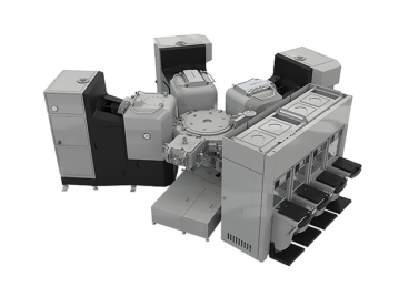
At Beneq, we engineer the SiC interface with a 3-step Atomic Layer Deposition workflow for extracting the best performance from SiC MOSFET devices.
- Efficient, in-situ plasma precleaning process for the SiC surface to remove the native oxide and reduce interface traps with minimum surface damage.
- ALD growth of a SiO2 interfacial layer to create a clean, defect-free SiC-dielectric interface.
- Final passivation layer by ALD (dielectric deposition).
By replacing the oxidation process with a high-quality, ALD-fabricated gate dielectric, the resulting device exhibits reduced Ron, reduced Dit, lower hysteresis, and higher mobility.
Contact us to learn how our ALD solutions can help improve your SiC power devices!