ALD for moisture protection
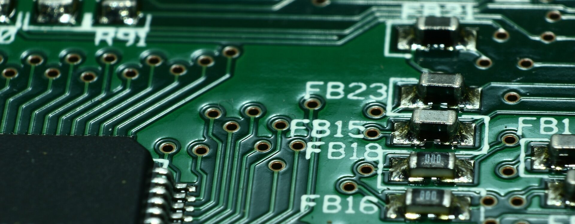
Wherever we have electronics, we have circuit boards (CB). The ever-increasing demand for higher performance of electronics in more demanding environmental conditions is pushing the limits of current circuit board packaging technologies’ performance. If the circuit boards are designed and assembled well, they should endure in the environment they are intended to work in. However, in new challenging environments, CBs may need maintenance more often than would be desirable. Usually moisture and temperature are the greatest threats to circuit boards and they accelerate failure generation.
Electrochemical migration (ECM) is one nasty phenomenon in circuit assemblies. What it needs to be manifested is moisture, electrical current and conductive residues. When an electronic product is in use, there is obviously current available for the ECM to happen. To effectively prevent ECM, one needs to either eliminate moisture or the residues.
Eliminate damage caused by moisture
Some applications are of the kind that the maintenance or repairs of the installed electronics can be extremely expensive, difficult, or both. Imagine a sensor at the bottom of the ocean monitoring a process. The cost of the sensor component could be in the hundreds of euros, if we are talking about an expensive high-end sensor, with no other electronics included. The changing or repair costs for the sensor could be anywhere from a couple of thousand to over ten thousand euros. Not to mention the time and money lost if the process needs to be halted.
Imagine if you could completely eliminate the need of maintenance. This means that instead of changing the sensor for example twice a year, you could use the same sensor for the whole lifetime of the application. Even if the sensor’s price would go up because of, e.g., an extremely durable coating applied on it, you can easily calculate the benefits and conclude that the slight increase in sensor price would easily be worth it.
Save the day with Atomic Layer Deposition (ALD)
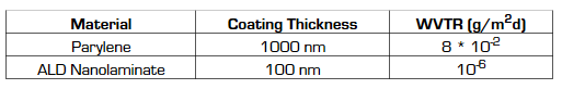
For demanding applications where humidity induced failures are simply not accepted, atomic layer deposition (ALD) thin films could save the day. With a nanolaminate ALD film, extremely low values for water vapour transmission rate (WVTR) can be achieved. See the comparison example below.
The ALD process is a vacuum process, where precursors are introduced to the substrate sequentially. Because the ALD process is based on chemical reactions between the different precursors on the surface of the substrate, the thickness of the coating can be controlled by the number of precursor cycles. The design of the cycle amounts and order is called a recipe. Typically each cycle grows one atomic layer of the material.
The coating process itself is relatively simple. The products are inserted into the ALD chamber, which is transferred into the ALD reactor. After that, the chamber is pumped into vacuum and heated. Then the process is started, and precursor cycles are performed according to the recipe. A typical process lasts about 8 hours and can be performed in temperatures under 100°C.
You can fit from several hundred to thousands of PCS of, e.g,. USB stick size into a typical ALD chamber. This significantly drives down the cost of deposition per PCB, making ALD a commercially attractive process for a broad variety of demanding environmental protection applications.
As can be seen from the table above, an extremely thin ALD coating is enough to block moisture penetration efficiently. If mechanical strength is needed for the film, the coating can be made thicker.
Let ALD take away your worries of failing electronics in humid environments!