ATOMIC LAYER DEPOSITION
Beneq’s Guide to ALD Acronyms
The field of Atomic Layer Deposition has grown substantially in the past 50 years resulting in numerous innovative modifications of the traditional thermal process. Each new sub-technique has its own acronym and can be overwhelming for individuals and industries new to the field. Learn here about the types of ALD, how they differ and other ALD-related slang.
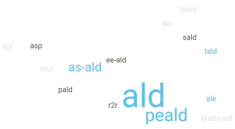
Beneq’s Guide to ALD Acronyms
ALD used to be called ALE, but that ALE isn’t the same as the new ALE? What’s the difference between PEALD and PALD? I thought ASP was a biblical snake?
Are you new to ALD and feeling overwhelmed by all the acronyms? Don’t fret – Beneq is here to help.
In the last 50 years, Atomic Layer Deposition, or ALD, has evolved far past its humble thermal roots in Finland. All across the world, researchers and industrialists are finding new and innovative ways to use ALD by changing the reactants, substrates, or movement of the two relative to each other. This rich research environment, coupled with intense industrial interest, has produced a large web of ALD outshoots, each with its own characteristics, and each with its own acronym.
To help you navigate the wonderful world of Atomic Layer Deposition, here is Beneq’s Guide to ALD Acronyms (and other ALD slang).
Types of Atomic Layer Deposition
ALD – Atomic Layer Deposition
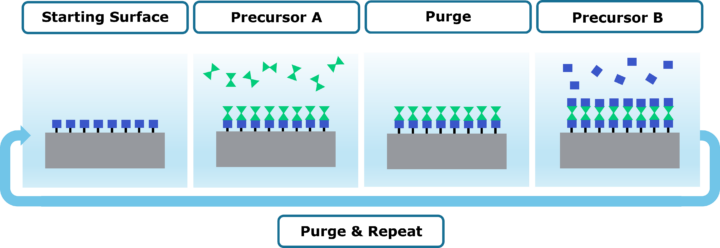
If you are here, then you are likely familiar with this acronym. When using this, you are often referring to thermal ALD. This is the most basic type of ALD where precursors are sequentially dosed to the substrate surface and reactions are driven primarily by temperature. This is the springboard from which all other types of ALD were invented.
Read more about Atomic Layer Deposition >
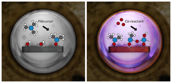
PEALD – Plasma-Enhanced Atomic Layer Deposition
This type of ALD utilizes plasma as the co-reactant for a deposition. It was originally commercialized in the 2000’s to aid in the deposition of titanium and tantalum films for trench barrier applications . PE-ALD tends to be slightly less isotropic than thermal ALD due to the directionality of the substrate, but it works well for low temperature depositions and provides new parameters to play with to tune material properties.
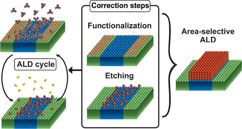
AS-ALD – Area-Selective Atomic Layer Deposition (aka ASD, Area-Selective Deposition)
This is one of the hottest new topics in ALD. AS-ALD exploits clever surface chemistry and growth mechanisms to deposit material on one area and not on another. This can be achieved by inhibiting growth on one surface with molecules, like self-assembled monolayers, or leverage one chemistry’s growth rate differences on separate surfaces, e.g., metal surface vs oxide. Harnessing AS-ALD will allow bottom-up nanofabrication by simply depositing materials where you want them, instead of having to do costly and time-consuming patterning steps. AS-ALD has even garnered its own annual event now among the ALD community.
Well-known groups working on AS-ALD include:
Mikko Ritala (University of Helsinki), Stacey Bent (Stanford University), Greg Parsons (North Carolina State University), Han-Bo-Ram Lee (Incheon National University), Adrie Mackus (Eindhoven University)
EE-ALD – Electron-Enhanced Atomic Layer Deposition
This type of ALD uses an electron beam to modify a surface to enhance its reactivity. It was pioneered by the George Group in Colorado to use for bottom-up fills of trenches and vias with metal films. One such mechanism uses so-called “electron stimulated desorption” to desorb hydrogens from a Si surface to open new reactive sites. The technique has been used to deposit films of Si, BN, Co, TiN and SiO2.
Selected Publications
J.K. Sprenger et al. Electron-enhanced atomic layer deposition of silicon thin films at room temperature – J. Vac. Sci. Technol. A 36, 01A118 (2018)
Z.C. Sobell et al. Electron-Enhanced Atomic Layer Deposition of Titanium Nitride Films Using an Ammonia Reactive Background Gas – Chem. Mater. 2022, 34, 21, 9624–9633
PALD – Powder Atomic Layer Deposition
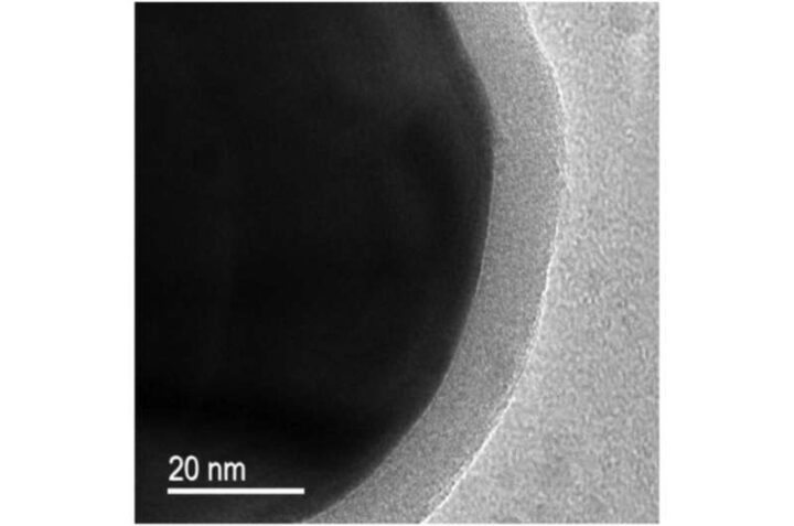
This is one substrate specific type of ALD. It is basically the use of ALD to coat powders with thin films. PALD requires some specialized equipment, like fluidized bed reactors, to expose all surface areas to the reactants. PALD has been used to coat electrode materials with protective coatings and to improve the flowability of pharmaceutical powders.
Groups specializing in PALD include:
Ruud van Ommen (TU Delft), Al Weimer (CU Boulder), Peter Stair (Northwestern)
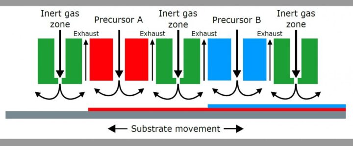
SALD – Spatial Atomic Layer Deposition
Spatial ALD is ALD where the substrate moves relative to the reactants instead of introducing the reactants one-by-one to the substrate surface. There are many types of spatial ALD, but they all tend to have much faster growth rates than temporal ALD because multiple surfaces can be coated simultaneously. In some SALD configurations, like the Beneq C2R, up to 1 micron/hour of material can be deposited, about 100x faster than thermal ALD.
Learn more about SALD in Chapter 7 of the Evolution of the ALD Reactor >
R2R ALD – Roll-to-roll Atomic Layer Deposition
This is a type of spatial ALD specifically for web-based substrates. Roll-to-roll reactors unwind a roll of flexible material through reaction zones and spool it up on the other end. This type of ALD is well-known for coating battery electrodes or flexible electronics.
Check out the Genesis ALD R2R tool >
FEALD – Flash-Enhanced Atomic Layer Deposition
Flash-Enhanced ALD exposes the surface to periodic millisecond flashes of light during the deposition. By doing so, the flash lamp heats the surface of the substrate to high enough temperatures that provide additional thermal energy to the surface reactions. By doing this, materials that can only be deposited at high temperatures could be made on thermally sensitive substrates at low temperatures. It could also be used for single-source depositions of metals. The process may be used to anneal the film each cycle rather than doing high temperature annealing after a film has been completed.
Selected Publications
T. Henke et al. Flash-Lamp-Enhanced Atomic Layer Deposition of Thin Films – 2014 ECS Trans. 64 167
Photo-ALD – Photo-assisted Atomic Layer Deposition
Photo-ALD, like FEALD, is a relatively unexplored deposition method utilizing light to provide energy for a reaction. Photo-ALD uses pulses of UV or visible light at the substrate surface allowing for single-source ALD processes, quicker reaction sequences and depositions on thermally sensitive substrates.
Selected Publications
V. Miikkulainen et al. Photo-Assisted ALD: Process Development and Application Perspectives – 2017 ECS Trans. 80 49
Other ALD-Related Acronyms
ALE – Atomic Layer Epitaxy OR Atomic Layer Etching
This one can be confusing. ALE was the original acronym for ALD but drove the epitaxy folks a bit crazy. To avoid confusion, Suntola’s ALE was changed to ALD. Thankfully, we found another use for it once etching came on the scene. Atomic layer etching had long been used in the semiconductor world by modifying the surface than bombarding with ions. ALD’s true reversal, thermal ALE, was not invented until 2016 in the George Group. Now ALE stands side-by-side ALD at the annual conference.
ASP – Atomic Scale Processing
This is an emerging acronym to encompass the tool box of techniques that manipulate material on the atomic scale. Atomic Scale Processing would include the likes of ALD, ALE, AS-ALD, etc. Even some events have adopted this type of lingo, like the German-led ALPIN even (Atomic Layer Processing Innovation Network).
MLD – Molecular Layer Deposition
This is the hybrid/organic analog of ALD. Rather than depositing binary inorganic materials, molecular layer deposition has been used to create inorganic-organic hybrid films, as well as all organic films. One major application for MLD is the deposition of alucone (hybrid organic-Al2O3 film) for coating Si battery anodes. When Si inevitably expands from lithiation, alucone offers the robust protection of alumina, while imparting flexibility with the organic interlayers.
VPI & SIS – Vapor Phase Infiltration & Sequential Infiltration Synthesis
While there are some nuanced differences, these two processes are similar derivations of ALD to form inorganic materials inside polymer substrates. One still uses an ALD-like process where two reactants are introduced sequentially, but the metal precursor is first allowed to diffuse inside the polymeric material before interacting with the co-reactant. These could be easier processes to make hybrid films than doing MLD since MLD already can suffer from diffusion effects.