GaN POWER
ALD Solutions for Gallium Nitride Power Devices
Gallium nitride (GaN) is the chosen material for next-generation power devices due to its high breakdown strength, high electron mobility and lower power consumption. GaN power devices are rapidly replacing traditional silicon-based electronics for low voltage applications. High electron mobility transistors (HEMTs) show up to 1000 times more efficient electron conductivity than Si, and can be manufactured smaller and at lower costs.
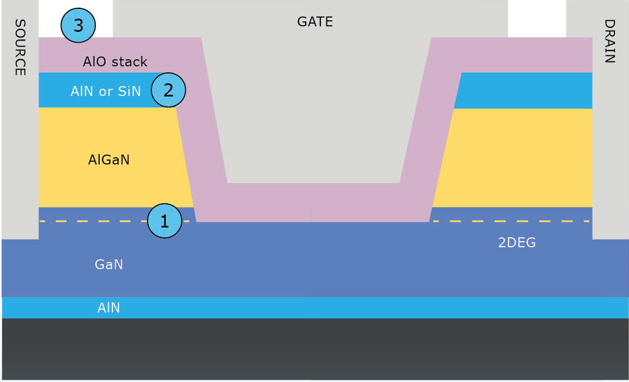
Reducing density of interface traps (Dit) in GaN power devices
Despite the superior performance of GaN power devices, the unstable interfacial GaOx produces numerous interface traps, significantly degrading device performance. At Beneq, we offer a 3-step Atomic Layer Deposition workflow for extracting the best performance from your power devices (shown below):
- Efficient, in-situ plasma precleaning process for the GaN surface to remove the native oxide and reduce interface traps with minimum surface damage.
- ALD growth of a nitride interfacial layer to create a clean GaN-dielectric interface with improved lattice match.
- Final dielectric capping layer by ALD to prevent oxidation of the interfacial layer.
Other thin film solutions for GaN power devices include:
- Conformal gate dielectric deposition
- Atomically controlled surface passivation and capping
- High-quality nucleation and buffer layers
- Low-temperature, conformal stacks for encapsulation