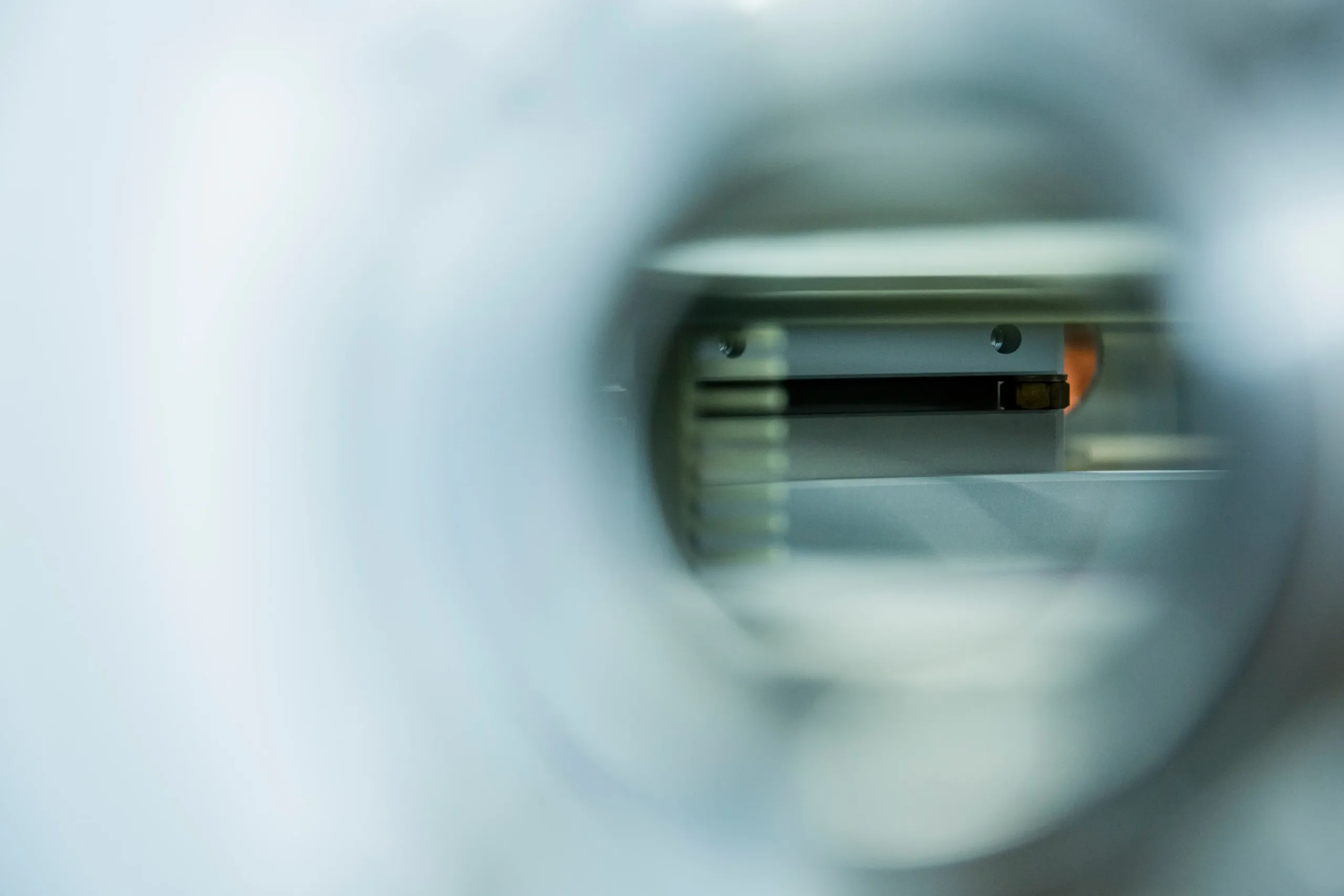
Operating at up to 40 wafers/hour with three processing modules, the Beneq Transform® changed previously held user perceptions of low atomic layer deposition (ALD) throughput.
As of November 2021, Beneq has seen higher than expected demand for both the Transform® and Transform® Lite product configurations across key customer regions such as EU, Japan, China, Taiwan and USA.
“Customers are increasingly choosing the Beneq Transform® to support the development of new technologies and significantly enhance the performance and durability of their products. We are very proud of the reputation it has gained in different markets. This growing acclaim further solidifies our mission to be dedicated to the success of More-than-Moore device makers,” states Patrick Rabinzohn, Vice President, Semiconductor ALD at Beneq.
Taguhi Yeghoyan, PhD, a Technology & Market Analyst for Semiconductor Manufacturing at Yole Développement (Yole) describes the burgeoning demand for solutions like the Beneq Transform®: “Propelled by 200mm wafer production, the ALD equipment market for More-than Moore device applications is surging with a 12% compound annual growth rate and is set to be worth $680.5 million by 2026.”
“As of 2020, 300mm ALD platforms already held majority of the equipment market share for More-than-Moore devices. In the coming years, 200 mm ALD platforms should become more competitive due to the steep ramp-up in wafer production for applications such as MEMS and sensors as well as compound semiconductor-based power, RF, LED and photonics devices. BENEQ will benefit from these dynamics, thanks to its Transform® ALD cluster tool,” asserts Yeghoyan.
Due to its versatility in offering both thermal batch and plasma processing modules, the Beneq Transform® is widely deployed from corporate R&D to foundry manufacturing of up to 200mm wafer devices. It offers fully automatic and high throughput production of, for example, power devices, RF filters, RF ICs, MEMS, image sensors, LEDs and OLED devices.
Typical applications for the Beneq Transform® include the following:

In October 2020, Beneq opened a new cleanroom at its facility in Espoo, Finland, to support the production of Beneq Transform® (ISO 7) and semiconductor ALD applications (ISO 5).
Beneq plans to further expand its ALD product portfolio to serve even more semiconductor customers over the next months.
Learn more about Beneq Transform: /en/products/semiconductors/transform
More information:
Lie Luo, Head of Marketing, lie.luo@beneq.com
About Beneq
Beneq is the home of atomic layer deposition. In 1984, we established the world’s first industrial production using ALD. Today, we lead the market with products for R&D (TFS 200, TFS 500, R2), semiconductor device fabrication (Transform®), 3D and batch production (P400A, P800, P1500), ultra-fast spatial ALD (C2R), and roll-to-roll ALD (Genesis).
Beneq’s unique Development Service simplifies customer adoption and proof-of-concept for new ALD processes, while our Coating Service cuts down time to market by outsourcing state of the art ALD production. Our team of engineers and experts is dedicated to making ALD tools accessible for researchers.
The Beneq Transform® has revolutionized ALD cluster tools for More-than-Moore semiconductor markets in the EU, the US and Asia since its launch in 2019. Based on its rapid success, Beneq plans to expand its portfolio to cater to the needs of even more semiconductor manufacturers.
Operating at up to 40 wafers/hour with three processing modules, the Beneq Transform® changed previously held user perceptions of low atomic layer deposition (ALD) throughput.
As of November 2021, Beneq has seen higher than expected demand for both the Transform® and Transform® Lite product configurations across key customer regions such as EU, Japan, China, Taiwan and USA.
“Customers are increasingly choosing the Beneq Transform® to support the development of new technologies and significantly enhance the performance and durability of their products. We are very proud of the reputation it has gained in different markets. This growing acclaim further solidifies our mission to be dedicated to the success of More-than-Moore device makers,” states Patrick Rabinzohn, Vice President, Semiconductor ALD at Beneq.
Taguhi Yeghoyan, PhD, a Technology & Market Analyst for Semiconductor Manufacturing at Yole Développement (Yole) describes the burgeoning demand for solutions like the Beneq Transform®: “Propelled by 200mm wafer production, the ALD equipment market for More-than Moore device applications is surging with a 12% compound annual growth rate and is set to be worth $680.5 million by 2026.”
“As of 2020, 300mm ALD platforms already held majority of the equipment market share for More-than-Moore devices. In the coming years, 200 mm ALD platforms should become more competitive due to the steep ramp-up in wafer production for applications such as MEMS and sensors as well as compound semiconductor-based power, RF, LED and photonics devices. BENEQ will benefit from these dynamics, thanks to its Transform® ALD cluster tool,” asserts Yeghoyan.
Due to its versatility in offering both thermal batch and plasma processing modules, the Beneq Transform® is widely deployed from corporate R&D to foundry manufacturing of up to 200mm wafer devices. It offers fully automatic and high throughput production of, for example, power devices, RF filters, RF ICs, MEMS, image sensors, LEDs and OLED devices.
Typical applications for the Beneq Transform® include the following:

In October 2020, Beneq opened a new cleanroom at its facility in Espoo, Finland, to support the production of Beneq Transform® (ISO 7) and semiconductor ALD applications (ISO 5).
Beneq plans to further expand its ALD product portfolio to serve even more semiconductor customers over the next months.
Learn more about Beneq Transform: /en/products/semiconductors/transform
More information:
Lie Luo, Head of Marketing, lie.luo@beneq.com
About Beneq
Beneq is the home of atomic layer deposition. In 1984, we established the world’s first industrial production using ALD. Today, we lead the market with products for R&D (TFS 200, TFS 500, R2), semiconductor device fabrication (Transform®), 3D and batch production (P400A, P800, P1500), ultra-fast spatial ALD (C2R), and roll-to-roll ALD (Genesis).
Beneq’s unique Development Service simplifies customer adoption and proof-of-concept for new ALD processes, while our Coating Service cuts down time to market by outsourcing state of the art ALD production. Our team of engineers and experts is dedicated to making ALD tools accessible for researchers.


