Atomic Layer Deposition (ALD) is known in the electronics industry as an enabler for the scaling of logic and memory semiconductor devices. Ultimately, this scaling leads to performance improvement of devices such as dynamic random-access memory (DRAM), advanced fin field effect transistor (FinFET) and Gate All Around transistors. ALD is now percolating into More-than-Moore (MtM) device production, again enabling novel architectures, materials, and performance improvements. Examples include GaN and SiC transistors, in particular GaN High Electron Mobility Transistors (HEMTs) and SiC trench metal oxide semiconductor FETs (MOSFETs), piezoelectric microelectromechanical systems (MEMS) and radiofrequency (RF) devices or compound semiconductor mini-light emitting diodes (LEDs) and micro-LEDs.
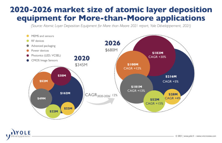
Besides the technical benefits that ALD offers, surging ALD equipment sales are propelled by fab capacity expansions worldwide. Forecasts expect the ALD equipment market for MtM devices to grow in the coming years with a 12% Compound Annual Growth Rate from 2020-2026 (CAGR2020-2026) reaching $680.5M in 2026.
You can find detailed know-how, market, and ecosystem overview of ALD equipment dedicated to MtM device production in the technology and market report Atomic Layer Deposition Equipment for More than Moore 2021, published by Yole Développement (Yole). Among the featured equipment manufacturers, Beneq is gaining momentum in the MtM space with a rapidly growing equipment lineup.
Taguhi Yeghoyan, Ph.D., Semiconductor Manufacturing Technology and Market Analyst at Yole, had a discussion with Patrick Rabinzohn, Ph.D., VP of the Semiconductor ALD Business Unit at Beneq. Below, read their exploration of the increasing adoption of ALD processes and ALD equipment in the serial production of MtM devices.
Taguhi Yeghoyan (TY): You have had an impressive career, holding high-level positions at some of the largest ALD companies. Now you are contributing to Beneq’s growth. Could you introduce Beneq and the company’s qualities that made you choose it?
Patrick Rabinzohn (PR): Thank you, Taguhi. I am indeed enjoying a long career in the semiconductor industry and always found it quite motivating. Beneq is the home of ALD and has ALD in its DNA. In fact, the very first industrial application of ALD was done in 1984 here on electroluminescent displays, at the same location where Beneq still is headquartered today! My collaboration with Beneq started in 2017. I could rapidly influence the strategy of the company until we decided to focus part of Beneq’s ALD equipment business on semiconductor as of 2019. Since then, Beneq has experienced both rapid transformation and huge business growth both ALD equipment for semiconductor markets within my business unit and other markets with our advanced ALD business unit.
ALD processes and equipment have been used in logic and memory device High Volume Manufacturing (HVM) for almost 20 years now. In the MtM space, ALD is used primarily for Complementary Metal Oxide Semiconductor (CMOS) Image Sensor (CIS) production while other MtM devices, such as power, RF, MEMS, and photonics, are just starting to embrace it.
TY: What are the challenges for ALD adoption in MtM device serial production? How can ALD equipment vendors, such as Beneq, help foundries?
PR: First of all, it has been our strategy to focus on MtM in order to establish Beneq first as a successful newcomer in the semiconductor equipment industry, while transitioning to the rising challenger we are today. The challenges for adoption of ALD in the production of MtM devices are twofold. First MtM devices need to face technology inflections for which ALD becomes a must. Second, generally the throughput of ALD is perceived to be too low or its cost of ownership too high. These challenges are not specific to MtM and used to be the same in memory and logic. Regarding the first challenge, ALD is the way to go when surface and interface control is critical and/or films with high quality, conformality and uniformity are needed. When it comes to throughput, one order-of-magnitude improvement is made possible thanks to our advanced batch thermal ALD technology. This is sometimes called mini-batch, and is designed for standard wafer handling systems and advanced cluster tool design, incorporating rapid pre-heating for manufacturing worthiness.
ALD is known for the deposition of excellent quality nanometric thin films, which can compete with thicker Chemical and Physical Vapor Deposition (CVD and PVD) coatings. However, CVD and PVD processes are more mature with equipment optimized for HVM.
TY: Would you agree that ALD can replace CVD and PVD processes in the future? What are the blocking points?
PR: Indeed, ALD is replacing or complementing CVD and PVD processes, and this will continue in the future, where they fail to meet the inflection point. This trend applies to multiple market segments such as power devices, compound semiconductors, including RF, VCSEL, LED/micro-LED, light detectors and photonics, micro-OLEDs, RF filters, image sensors, MEMS and actuators. It also applies to many ALD functionalities such as high-k dielectrics, surface passivation, nucleation and seed layers, chemical barriers, encapsulation moisture barriers or anti-reflective coating. One factor is limiting the replacement of CVD and PVD. This is the thickness one can deposit by ALD in a production mode. Our state of the art mini-batch technology has pushed this limit from about 10 nm to 100 nm. Also, for the fact that high quality ALD does not require as thick a film as CVD for example, a broad range of CVD and PVD processes within the MtM space will increasingly move over to ALD going forward. A remaining bottleneck is the limited availability of ALD chemistries and processes for the deposition of metals or conductive films at industrial scale.

TY: Related to the previous questions, could you share with our readers the recent advancements in ALD equipment technology dedicated to MtM devices in general, especially for Beneq?
PR: Sure. Beyond the state-of-the-art mini-batch technology, there are two other technologies which are enabling ALD for MtM devices. One is the capability to integrate plasma ALD and thermal batch ALD process modules on the same platform, thus widening the scope of applications at meaningful throughput. This enables us to have the versatility to adapt to different capacity, product and applications mix. Another capability is that our single wafer process module can run plasma and/or thermal ALD processes in-situ. This is another contributor to the versatility required for MtM.
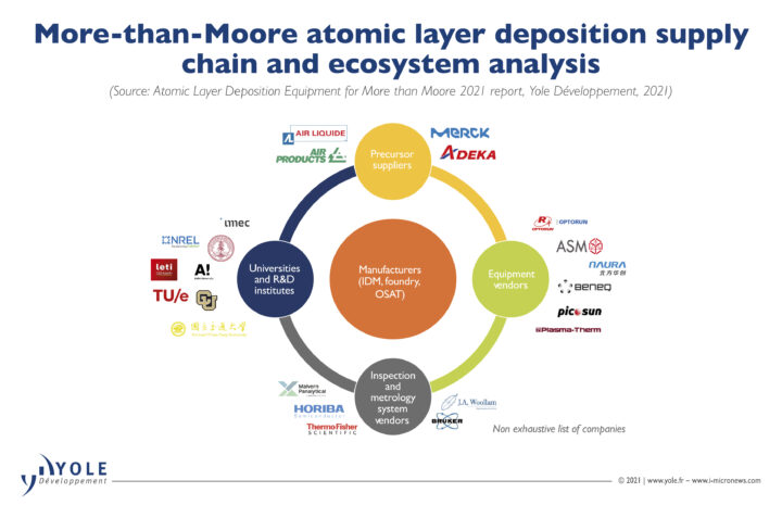
Despite some ALD adoption for MtM device production, the ALD process is still developed largely in collaboration with academics and R&D institutes. Often, material suppliers, equipment subpart and tool vendors, and inspection and metrology system vendors contribute. Beneq is an active participant in this worldwide cooperation.
TY: Could you comment on how equipment makers, in particular Beneq, interact with the supply chain and contribute to ALD process development worldwide?
PR: This is a complex question. Let me first comment on the ALD process. It is clear that ALD has attracted and continues to attract more academic research than other thin film deposition technologies. This might be due to the atomic scale nature of ALD which is more accessible for research. Beneq has a strong position in academic research thanks to our well established TFS tool and our newest R2 tool. Obviously, this supports collaboration for example through sponsoring of students or joint publications. Importantly, similarly to other technologies, the development or customization of ALD applications on relevant devices and structures often requires close collaboration with our customers and research and technology organizations (RTOs). This is our primary focus and an integral part of our sales process ever through development services or demonstrations. Obviously other collaborations exist when mutually beneficial, for example with materials suppliers.
In addition to ALD community collaborations, the number of ALD equipment vendors is growing worldwide, and the business is becoming highly competitive. Moreover, this trend is strengthened by governments’ ambitions to build local supply chains.
TY: Considering that most MtM devices concerned are produced in the East Asia region, how can equipment makers based elsewhere such as Beneq compete?
PR: It is a good sign that competition among ALD equipment vendors is growing, especially in the MtM market. Though Europe, US and Japan have pioneered most of the development and production of MtM devices so far, volume manufacturing started to be moved to Taiwan and to some extent Southeast Asia (SEA) a few years ago for example for LEDs or some RF devices. More recently China is adding to that trend. Beneq has been present in China since its inception and our current investor and partner brings significant industrial leverage for localization of the supply chain. Furthermore, earlier this year we established Beneq KK in Japan as well as partnerships in Taiwan and SEA.
The ALD equipment market can be divided into equipment serving 200 mm and 300 mm wafer volume processing, with an estimated adoption rate of 28% and 72% in 2020, respectively. In the coming years, we expect a relatively steeper ramp-up in 200 mm wafer production, reaching 44% of total production by 2026.
TY: We expect that many 200 mm ALD platforms will be required to satisfy the needs of the industry. Such platforms are Beneq’s specialty. Could you share your point of view with us?
PR: As you noted, 300 mm ALD equipment is the largest part of the current MtM market. This is essentially because multiple ALD applications have enabled CIS and ALD is the production tool of record in high volume manufacturing. However, early on this market was captured by industry leading OEMs focused on leading edge technologies and Moore’s law. Beneq and other ALD equipment suppliers did not participate. Over the last one to two years opportunities for ALD have grown in other market segments such as power, micro-OLEDs and micro-LEDs as well as advanced packaging. For this reason, 300 mm becomes a lower hanging fruit for many original equipment manufacturers (OEMs) such as Beneq.
Despite the steep ramp-up of 200 mm wafer production volume, 300 mm wafers will remain predominant during the coming years with an expected adoption of 56% by 2026. The 300 mm wafer volume is driven by CIS and silicon power device HVM. Hence, more and more 200 mm ALD equipment providers may upgrade their systems to handle 300 mm wafers.
TY: What is the differentiator for ALD equipment users among existing 300 mm platforms and the new lineup from traditionally 200 mm ALD equipment providers? Could you share with our readers Beneq’s plans regarding the 300 mm platform?
PR: We believe that in the MtM space, 300 mm ALD equipment users have similar requirements to 200 mm ALD equipment users. Affordable and versatile ALD equipment is their motto. The mini-batch technology, the integration of plasma ALD and thermal batch ALD process modules on the same platform and, when meaningful, the capability to run plasma and/or thermal ALD processes in-situ remain key differentiators for 300 mm MtM. We at Beneq have now expanded our semiconductor equipment portfolio to 300 mm based on similar advanced cluster tool designed with standard wafer handling systems and incorporating our rapid pre-heating technology. Nevertheless, as you observed, 200 mm MtM technologies and markets are expected to go through steep growth in the coming years. In particular smaller wafers, down to 3”, driven by compound semiconductors, must not be neglected in equipment portfolios. To learn more about our latest new product announcements, look Here.
Interviewee

Patrick Rabinzohn, Ph.D., is Beneq’s VP of the Semiconductor Business Unit. He has 40 years of semiconductor industry experience across the Semiconductor, Semiconductor Equipment and Materials markets and has extensive knowledge of Equipment, Process, Process Integration and Technologies. Prior to Beneq, he held several high-profile roles, including CTO for IoT/MEMS and Advanced Packaging at Lam Research, General Manager at Intermolecular, Managing Director for Microelectronics at Alchimer, and CTO Europe at Applied Materials. He graduated from Ecole Superieure d’Electricite (Supelec) and received a Ph.D. in Materials Science from Paris University.
Interviewer

Taguhi Yeghoyan PhD., is a Technology & Market Analyst, Semiconductor Manufacturing at Yole Développement (Yole), within the Semiconductor, Memory & Computing division.
Taguhi’s mission is to follow the semiconductor industry and its daily evolution. Based on her expertise in this field, especially on the semiconductor value chain, processes, materials, equipment, and related applications, Taguhi produces technology & market reports and is engaged in dedicated custom projects.
Prior to Yole, she worked in world-class European research centers and laboratories, including imec (Belgium), LMI (Lyon, France), and LTM at CEA Leti (Grenoble, France). During her career, Taguhi has authored or co-authored one patent and more than nine papers.
Taguhi graduated from Wroclaw University of Technology (Poland) and the University of Lyon (France). She also completed her Ph.D. in Material Science from the University of Lyon (France).