Radio frequency, or RF, devices operate on radio waves (20 kHz – 300 GHz) and can be split into two categories: integrated circuits (ICs) and filters. Although the two types differ greatly in their function, both encounter interfacial challenges which can impact their performance. For example unstable surface oxides, e.g. Ga2O3, make high quality passivation layers critical for the operation of RF ICs. RF filters can benefit from improved bonding strength and corrosion resistance on electrodes.
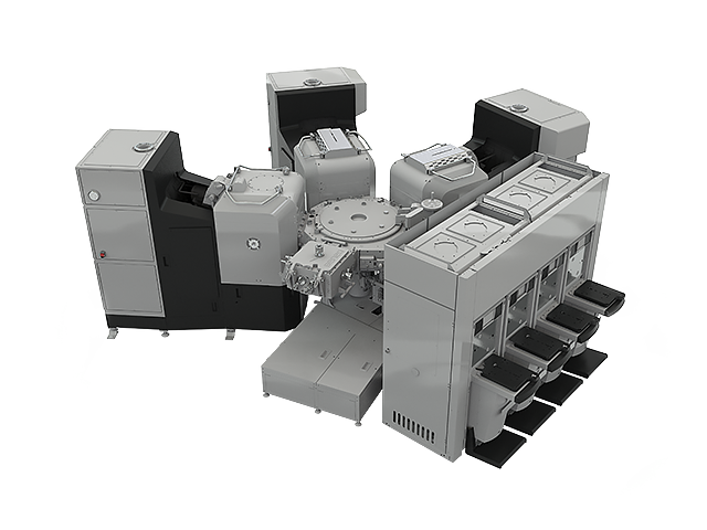
At Beneq, our Atomic Layer Deposition processes deposit ultra-thin and pinhole-free films with precision thickness control, high breakdown voltage and unparalleled step coverage. Our batch manufacturing cluster tools feature both thermal and plasma ALD, offering a range of thin film solutions for RF devices. Explore our solutions for RF ICs and filters below.
ALD SOLUTIONS FOR RF DEVICES
Process Options
Thermal ALD
Plasma-Enhanced ALD
Materials
Al2O3, AlN, SiO2, Si3N4, HfO2, Ta2O5, TiO2, TiN
Substrates
GaN, SiC, GaAs, InP
3, 6, 8, 12″ wafers
Radio Frequency ICs
- High-k gate dielectric for HEMT devices and MIM capacitors
- Conformal surface passivation and capping layers
- Robust final passivation and encapsulation films
Radio Frequency Filters
- Encapsulation films against corrosion and piezo degradation
- Heat dissipation layer on IDTs
- ALD adhesion and stress compensation
- Conformal surface passivation on PE and IDT materials


