Beneq C2 wins Compound Semiconductor High-Volume Manufacturing Award
Increasing the capacity of Atomic Layer Deposition (ALD) equipment and moving ALD from research laboratories to industrial production has been a target of Beneq Thin Film Solutions for a long time. Lately, our focus has been on developing high-capacity ALD solutions for wafer processing in the semiconductor industry.
In November last year, Beneq launched Beneq C2, a cluster-compatible automated ALD system for industrial processing of wafers. It was received with great interest on the market and we have already shipped the first equipment sets to our customers with several new orders now in line.
Now, we are happy to announce that the revolutionary features of Beneq C2 and its deposition speed and capacity have been recognized by the industry experts too.
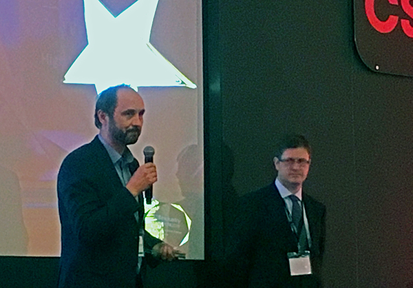
Beneq C2 receives the High-Volume Manufacturing Award in the CS International Conference
Beneq C2, the automated wafer ALD solution in Beneq’s cluster-compatible equipment portfolio, is the winner in the High-Volume Manufacturing category of the CS Industry Awards, where the industry experts have been able to vote for their favorites from a shortlist of nominees.
GaN (gallium nitride) high electron mobility transistors (HEMTs) have great potential for next generation energy-efficient power switching applications, but the devices require conformal high-quality dielectrics. High-capacity thermal and plasma enhanced ALD systems can create highly conformal dielectric layers that solve many challenges in high-throughput manufacturing of GaN HEMT devices.
Beneq C2 moves throughput of wafer ALD equipment to a completely of new level. It provides an optimal solution for high performance ALD on wafers in industrial applications in the emerging More than Moore semiconductor markets, such as Power and RF devices, RF and Piezoelectric MEMS, MEMS sensors and actuators, image Sensors, photonic integrated circuits, and OLED microdisplays.

CS AWARDS 2018 – Rewarding excellence, innovation and success
Sales of compound semiconductor chips are soaring. This is being driven by an uptake in solid-state lighting, rising revenues for smartphones, a build-out of capacity in optical networks, and greater use of energy-saving power electronics devices.
The CS Industry Awards have been established to showcase the success of companies within the compound semiconductor industry. The awards celebrate the leaders, the innovative engineers, and those that excel in meeting the needs of their customers in the semiconductor market.
Meet Beneq at CS International Conference, 10th-11th April in Brussels, Belgium
Beneq is present both in the exhibition and the conference at Compound Semiconductor International.
If you are at the event, make sure to go and listen to Beneq’s Mikko Söderlund’s presentation High-Capacity Wafer-Scale Solutions for More than Moore Applications on Tuesday April 10th at 13.45.
You can also find us from the exhibition hall during the event.
Should you want to book a meeting to hear the latest news about the ALD throughput revolution that is about to take place in the semiconductor industry, you can contact us through our event web page (see address below).
For ultra-fast ALD, the right address is Beneq.


