The CMOS Image Sensor (CIS) market keeps its momentum with double digit growth. Main and sub cameras for smartphone remain the leading application while automotive image sensors have quickly established themselves as second largest segment. These emerging opportunities have caused a paradigm shift from using vision for imaging to using vision for sensing and other interactive applications. Over the last decade new CIS technology has been developed to decrease pixel size while maintaining or enhancing electro-optical performance. A new CIS architecture, BackSide Illumination (BSI) technology, is a well-established alternative to the commonly used FrontSide Illumination (FSI) technology. BSI technology involves turning the image sensor upside down and applying color filters and micro lenses to the backside of the pixels, so that the sensor can collect light through the backside. BSI has a deep photo-diode and short optical path not shadowed by front side metal layers, leading to a higher Quantum Efficiency, Lower Crosstalk and higher Signal to Noise Ratio (SNR).
The challenge
The challenge lies in the ability to deposit a pinhole free, high breakdown voltage dielectric layer on the recessed MISHEMT structure. The conformality of the dielectric is key in achieving good device performance. In an E-mode MISHEMT, the addition of a gate dielectric may create a high-density of shallow and deep traps at the interface. Proper surface cleaning and pre-treatment as well as interfacial layer techniques are crucial for achieving a low density of interface traps.The BSI architecture requires an anti-reflective coating (ARC) at the backside Silicon surface to increase the quantity of photons absorbed in the photodiode. Moreover, this same layer or a separate additional layer, may serve to passivate the Si/SiO2 interface in order to reduce dark current via chemical and/or field effect passivation. Interface control and film quality of these layers set the performance of the image sensors.The challenge lies in the ability to deposit a pinhole free, high breakdown voltage dielectric layer on the recessed MISHEMT structure. The conformality of the dielectric is key in achieving good device performance. In an E-mode MISHEMT, the addition of a gate dielectric may create a high-density of shallow and deep traps at the interface. Proper surface cleaning and pre-treatment as well as interfacial layer techniques are crucial for achieving a low density of interface traps.
The customer
Manufacturers of CMOS Image Sensors seeking to decrease pixel size while enhancing performance to best in class aperture size and in low light situations for a wide range of applications including smartphones, automotive, security and medical.
Beneq solution
Through ALD, dielectrics such as Al2O3, AlON and HfO2 can be deposited as gate dielectrics with ideal conformality and repeatability down to thicknesses of a few monolayers. Batch thermal ALD capabilities enable high throughput whereas plasma pre-treatement and plasma ALD deposition support customization of the properties of the gate dielectric.
Al2O3 ALD is a well-established solution as passivation layer of Silicon. It is particularly well suited to improve passivation properties of BSI CIS ARC because 1) it is a low temperature process, 2) provides hydrogen to chemically passivate interface defects and 3) induces negative charge to induce field effect passivation. With a high refractive index Ta2O5 along with Al2O3 makes for an excellent stack as an anti-reflective coating. Both films can easily be grown with the same ALD tool either individually or sequentially. HfO2 ALD is an alternative material solution to Al2O3 ALD as field effect passivation layer. Additionally, the Si/ARC interface is an integral part of the stack. Control of the interface with/without SiO2 or another interfacial layer is critical.
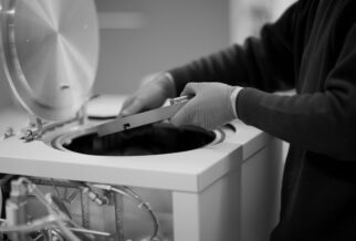
The BSI CIS ARC stack on active backside silicon needs to be made of very high-quality thin film and have very low level of density of defects. ALD provides the thinnest pinhole free oxide of any deposition method. Additionally, ALD is a relatively simple deposition methods which is fully compatible with standard silicon wafer processing. Beneq batch thermal ALD capabilities enable high throughput whereas plasma pre-treatment and Plasma ALD deposition support optimization of the interface.
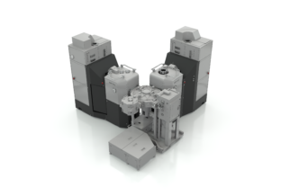
Beneq Transform™ automated ALD cluster tool is a flexible high capacity turn-key ALD solution. It is ideally suited for deposition of performance critical dielectric, passivation and barrier layers for More than Moore applications such as Power, MEMS, RF, LED, III-V, Photonics and beyond. Beneq Transform™ combines industry standard, ultra-clean and reliable cassette-to-cassette automation with Beneq proprietary single wafer and batch ALD process modules as well as additional PM’s for pre and post-treatments. Beneq ALD4 is compliant with ultra-clean requirements, SECS/GEM communication and SEMI S2 and S8 standards. Beneq C2 is a leading choice for MtM applications, featuring smallest footprint, highest capacity per cleanroom area, and lowest cost-of-ownership.
Through ALD, dielectrics such as Al2O3, AlON and HfO2 can be deposited as gate dielectrics with ideal conformality and repeatability down to thicknesses of a few monolayers. Batch thermal ALD capabilities enable high throughput whereas plasma pre-treatement and plasma ALD deposition support customization of the properties of the gate dielectric.
Beneq ALD batch cluster tools are flexible solutions for manufacturing gate dielectrics of GaN Power Devices In addition to gate dielectrics, the resistance of power devices to moisture intrusion is enhanced by ALD encapsulation using multilayer stacks or nano-laminates. The laminates may be a combination of various oxides deposited on temperatures as low as 70 C, depending on the materials involved. Finally, ALD AlN provides state of the art passivation of the GaN surface across the device.
Beneq Transform™ automated ALD cluster tool is a flexible high capacity turn-key ALD solution. It is ideally suited for deposition of performance critical dielectric, passivation and barrier layers for More than Moore applications such as Power, MEMS, RF, LED, III-V, Photonics and beyond. Beneq Transform™ combines industry standard, ultra-clean and reliable cassette-to-cassette automation with Beneq proprietary single wafer and batch ALD process modules as well as additional PM’s for pre and post-treatments. Beneq Transform™ is compliant with ultra-clean requirements, SECS/GEM communication and SEMI S2 and S8 standards. Beneq C2 is a leading choice for MtM applications, featuring smallest footprint, highest capacity per cleanroom area, and lowest cost-of-ownership.