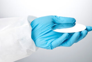
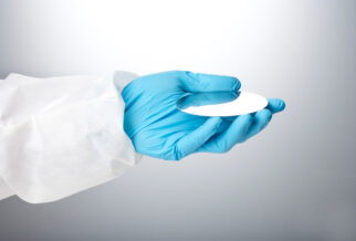
Products
Semiconductor Equipment
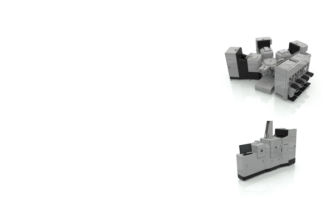
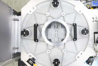
The Beneq Transform® is a new class of ALD cluster tool. It uniquely combines automation with both thermal batch and plasma enhanced ALD process modules. The Beneq Transform® offers unparalleled flexibility for processing sequences with multiple ALD process modules to meet wafer capacity. It is designed to be upgradable to meet growing volumes and new ALD processes.
BENEQ Transform®
The Beneq Transform® is a one-stop, production-ready ALD solution for power electronics, MEMS and sensors, RF, LED, photonics, and encapsulation applications. It offers both thermal and plasma ALD modules and is capable of single or batch processing. Its proprietary preheating module eliminates hours of waiting time and boosts throughput to a whole new level: 15 wafers per hour @50 nm Al2O3, in thermal mode. Throughput can be further increased by adding up to 2 more process modules, thermal or plasma.
See productBENEQ Transform® Lite
Maximize versatility as volume scales. The Beneq Transform® Lite offers the same thermal, plasma and preheating module as the larger Transform®. It works well for R&D, prototyping, as well as volume production. It is capable of surface pre-treatment and can coat substrate materials at wafer sizes from 3 to 8 inches. With the BENEQ Transform® Lite customers can now run several different ALD processes on multiple devices and applications, all on a single footprint!
See product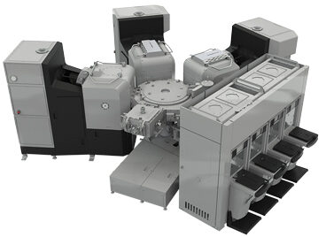
Beneq Transform® 300
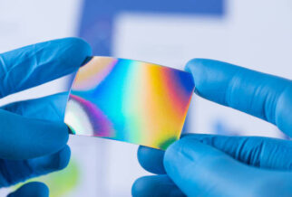
Beneq Transform® 300 is the only 300 mm ALD cluster tool combining thermal ALD (batch) and plasma ALD (single wafer) technologies to provide a highly versatile platform to IDMs and foundries. Transform® 300 is dedicated to a broad range of advanced thin-film applications from gate dielectric, including in high aspect ratio trenches, to anti-reflection coating, final passivation or encapsulation and beyond for high-volume manufacturing CIS, Power, Micro-OLED/LED, Advanced Packaging and other MtM devices.
See product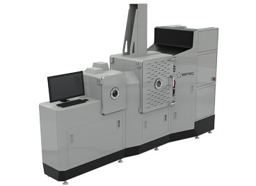
Beneq Prodigy™
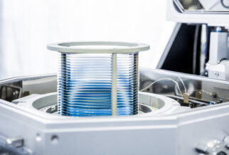
Beneq Prodigy™ sets a new standard for affordable volume manufacturing of compound semiconductors (CS) and MEMS devices with ALD. It is the ideal manufacturing solution for compound semiconductor including RF IC’s (GaAs/GaN/InP), LED, VCSEL and Light Detectors and for MEMS providing best-of-breed passivation and encapsulation films across various wafer sizes and types. Enjoy a simple, yet elegant, solution for enhancing device performance on 75-200 mm wafers with a low-cost batch tool with latest ALD technology.
See product