POWER DEVICES
Conformal ALD coatings for emerging GaN & SiC power devices
GaN and SiC are promising new materials for integrated power devices. Beneq Atomic Layer Deposition solutions can help solve the interfacial challenges associated with these electronics.
ALD FOR POWER DEVICES
High electron mobility and incomparable breakdown field make wide band-gap semiconductors, like GaN and SiC, the go-to materials for next-generation power devices. However, they suffer from drawbacks at their interface, including high interface trap density, current leakage and poor stability under voltage. Atomic Layer Deposition enables damage-free surface preparation of emerging GaN and SiC devices and traditional IGBTs, crucial for extracting the best electrical performance.
Process Options
Thermal ALD
Plasma-Enhanced ALD
Materials
Al2O3, AlN, SiO2, Si3N4, HfO2, Ta2O5, TiO2
Substrates
GaN, SiC, Si
3, 6, 8, 12″ wafers
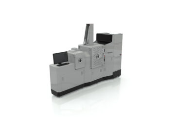
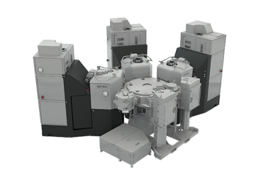
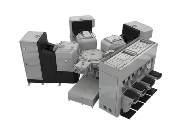
POWER DEVICE SOLUTIONS
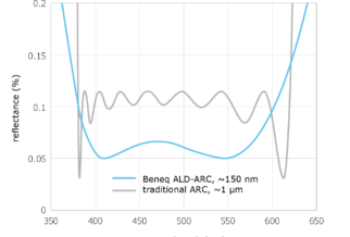
At Beneq, our ALD processes deposit ultra-thin and pinhole-free films with precision thickness control, high breakdown voltage and unparalleled step coverage. Our batch manufacturing cluster tools feature both thermal and plasma ALD, offering a range of thin film solutions for power devices including:
- High-k gate dielectric deposition
- Surface passivation for reduced interface traps
- Epitaxial nucleation or seed layers
- Wafer-level thin film encapsulation
GaN Power
Gallium nitride (GaN) is the chosen material for next-generation power devices due to its high breakdown strength, high electron mobility and lower power consumption. At Beneq, we use Atomic Layer Deposition workflows to reduce interface traps and extract the best performance from your GaN power devices.
SiC Power
Low ON resistance and high breakdown voltage, among other performance specifications, make SiC power devices a go-to material for high voltage uses, like power trains for railways and wind turbines. With ALD, we can engineer the SiC-oxide interface to increase the reliability of SiC MOSFET devices.