Wide bandgap (WBG) power semiconductor devices offer very significant energy efficiency gains in a wide range of applications including automotive, transportation, energy, industrial and consumer. WBG semiconductors such as Gallium Nitride (GaN) and Silicon Carbide (SiC) with their superior electrical properties are steadily replacing Silicon. GaN-based power devices are emerging as promising candidates for next generation high efficiency power converters owing to superior material properties such as high electric-field breakdown, high electron saturation velocity and high mobility. The dominant platform for developing commercial GaN power devices is based on lateral AlGaN/GaN heterojunctions grown on large-size, low-cost Silicon substrates.
For switching devices, normally OFF characteristics are preferred for safe operation of power electronic systems. Consequently, Enhancement mode (E-mode) GaN devices that can be switched on and off are desired. Among the two effective technologies to achieve E-mode operation with low ON resistance are the p-GaN gate HEMT and the Metal Insulator Semiconductor HEMT (MISHEMT) with fully recessed gate structure. MISHEMT exhibit large turn-on voltage operation and lower current leakage like Si and SiC power MOSFETs
The challenge
The challenge lies in the ability to deposit a pinhole free, high breakdown voltage dielectric layer on the recessed MISHEMT structure. The conformality of the dielectric is key in achieving good device performance. In an E-mode MISHEMT, the addition of a gate dielectric may create a high-density of shallow and deep traps at the interface. Proper surface cleaning and pre-treatment as well as interfacial layer techniques are crucial for achieving a low density of interface traps.
The customer
Manufacturers of power semiconductor devices developing solutions to extend the density by frequency performance window for a wide range of applications including automotive, communications, datacenters and consumer. In short, when the size-to-weight ratio matters.
Beneq solution
Through ALD, dielectrics such as Al2O3, AlON and HfO2 can be deposited as gate dielectrics with ideal conformality and repeatability down to thicknesses of a few monolayers. Batch thermal ALD capabilities enable high throughput whereas plasma pre-treatement and plasma ALD deposition support customization of the properties of the gate dielectric.
Beneq ALD batch cluster tools are flexible solutions for manufacturing gate dielectrics of GaN Power Devices. In addition to gate dielectrics, the resistance of power devices to moisture intrusion is enhanced by ALD encapsulation using multilayer stacks or nano-laminates. The laminates may be a combination of various oxides deposited on temperatures as low as 70c, depending on the materials involved. Finally, ALD AlN provides state of the art passivation of the GaN surface across the device.
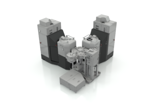
Beneq Transform™ automated ALD cluster tool is a flexible high capacity turn-key ALD solution. It is ideally suited for deposition of performance critical dielectric, passivation and barrier layers for More than Moore applications such as Power, MEMS, RF, LED, III-V, Photonics and beyond. Beneq Transform™ combines industry standard, ultra-clean and reliable cassette-to-cassette automation with Beneq proprietary single wafer and batch ALD process modules as well as additional PM’s for pre and post-treatments. Beneq Transform™ is compliant with ultra-clean requirements, SECS/GEM communication and SEMI S2 and S8 standards. Beneq C2 is a leading choice for MtM applications, featuring smallest footprint, highest capacity per cleanroom area, and lowest cost-of-ownership.