ADVANCED PACKAGING
ALD solutions for Thru Silicon Via and Chip Scale Packaging
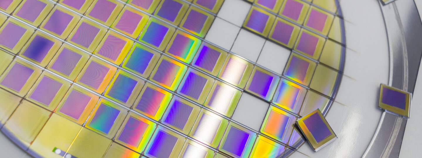
ALD provides conformal, dense and defect-free moisture barriers for hermetic sealing of dies on tape, post dicing, and CSP.
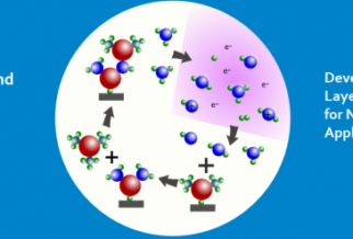
Thru Silicon Via (TSV) technology is the process of record in multiple advanced packaging approaches. The required high aspect ratio and the roughness of the sidewalls of the vias make ALD the leading candidate for deposition of the isolation layer as well as the barrier and seed layers of TSVs.
Another differentiated application of ALD in the field of advanced packaging is the hermetic sealing of dies on tape for Chip Scale Packaging (CSP) This is courtesy to the conformality of pin hole free ALD films deposited at very low temperature compatible with tapes and providing sufficient hermetic sealing.
Atomic Layer Deposition provides highly conformal moisture barriers with water vapor transmission rates as low as 1E-6 g/m2/day with films thinner than 50 nm. ALD encapsulation can be performed at low temperatures for damage-free encapsulation of sensitive electronic components. For packaging segments, ALD encapsulation can be applied at wafer level, on tape, as well as at package and module/board level to coat the device and any exposed electrical contacts.
ALD SOLUTIONS FOR ADVANCED PACKAGING
Process Options
Thermal ALD
Plasma-Enhanced ALD
Materials
For TSV: TiO2, TiN, TaN, Ru
For CSP: Al2O3, TiO2
Substrates
3, 4, 6, 8, 12″ wafers
Other ALD applications of moisture barriers include:
- Final passivation of semiconductors
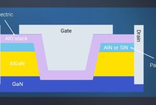
- GaN RF Devices
- LED-lighting devices
- VCSEL devices
Related products
You may be interested in
Related stories